SFB Colloquium
Dirac surface and interface states in topological crystalline insulators
| Datum: | 29.11.2018, 16:15 - 17:45 Uhr |
| Kategorie: | Kolloquium |
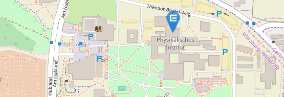
| Ort: | Hubland Süd, Geb. P1 (Physik), SE 2 |
| Veranstalter: | SFB 1170 ToCoTronics |
| Vortragende: | Prof. Dr. Tomasz Story - Institute of Physics, Polish Academy of Sciences, Warsaw |
Following the seminal theoretical proposal [1], a new class of 3D topological materials - topological crystalline insulators (TCI) - has been discovered by angle- and spin-resolved photoemission spectroscopy (ARPES) and scanning tunneling spectroscopy (STS) techniques. In contrast to model topological materials based on Bi and Sb chalcogenides, in TCI materials the topological protection of surface electronic states is warranted by crystalline (mirror-plane) symmetry [1]. The TCI states have been found in IV-VI narrow-gap semiconductors Pb1-xSnxTe (x=0.4-1) and Pb1-xSnxSe (x=0.18-0.4) for (001) and (111) crystal surfaces of both bulk crystals and epitaxial layers. These materials possess direct bulk energy gap at four L-points of the Brillouin zone and undergo a band inversion at specific Sn content and temperature. In the inverted bands regime one observes topological in-gap states forming 4 pairs of Dirac cones located across the edge of the (001) surface Brillouin zone. As the TCI states are protected by crystalline symmetry, lowering this symmetry by strain or crystal distortion qualitatively modifies the energy spectrum of topological states. This effect has been observed in Pb1-xSnxSe (001) by STS (in Landau quantization regime) [2] and ARPES experiments [3] revealing the gap opening in energy spectrum of two, out of four, Dirac cones.
In recent experimental studies of Shubnikov - de Haas and de Haas - van Alphen quantum oscillations the surface topological states were also observed for (001) surface of SnTe crystal [4]. By varying the angle between external magnetic field and the crystal we observed simultaneous contribution from neighboring (001) facets of the bulk crystal, thus demonstrating how the TCI topological states wrap the bulk of the crystal [4].
Variety of new proposals involving TCI materials relies on layered heterostructures and the effects of strain, hybridization or size quantization on topological properties. It requires detailed knowledge of the topological states at realistic surfaces with atomic steps or other defects as well as the topological interface states buried beneath trivial semiconductor caps. The unique electronic properties of atomic steps were recently demonstrated [5] with STM/STS technique, identifying 1D channel of high density electronic states along the odd-monolayer-high atomic steps at (001) surface of Pb1-xSnxSe. By in-situ capping the TCI surface of Pb0.7Sn0.3Se bulk crystal with an ultrathin topologically trivial layer of PbSe we carried out ARPES studies demonstrating the robustness of Dirac cones at Pb1-xSnxSe/PbSe interface and the important role of atomic steps that may induce an oscillatory collapse of the pair of split Dirac cones into a single one located at the edge of the Brillouin zone [6,7].
Our recent work concerning TCI SnTe nanowires, conductance tunneling spectroscopy of surface states [8] and alloy disorder effects in TCI transition [9] will also be presented.
[1] T.H. Hsieh, H. Lin, J. Liu, W. Duan, A. Bansil, L. Fu, Nat. Commun. 3, 982 (2012).
[2] I. Zeljkovic, Y. Okada, M. Serbyn et al., Nat. Mat. 14, 318 (2015).
[3] B.M. Wojek, M.H. Berntsen, V. Jonson et al., Nat. Commun. 6, 8463 (2015).
[4] K. Dybko, M. Szot, A. Szczerbakow et al., Phys. Rev. B 96, 205129 (2017).
[5] P. Sessi, D. Di Sante, A. Szczerbakow et al., Science 354, 1269 (2016).
[6] C.M. Polley, R. Buczko, A. Forsman et al., ACS Nano 12, 617 (2018).
[7] R. Rechciński, R. Buczko, arXiv:1808.0777.
[8] G. Mazur, K. Dybko, A. Szczerbakow et al., arXiv:1709.04000.
[9] A. Łusakowski, P. Bogusławski, T. Story, Phys. Rev. B 98 125203 (2018).


